
The Light-Powered Revolution That May End GPU Overheating
Coordenado por
**Prof. Aecio D’Silva, Ph.D.
A guide to how light-based processors work, who is building them, why they matter for AI, and how close they are to mainstream deployment.
SEO keywords: photonic computing, optical NPU, photonic AI accelerator, silicon photonics, AI data center cooling, GPU overheating, optical interconnect, light-based computing, AI inference chips, data center energy efficiency.
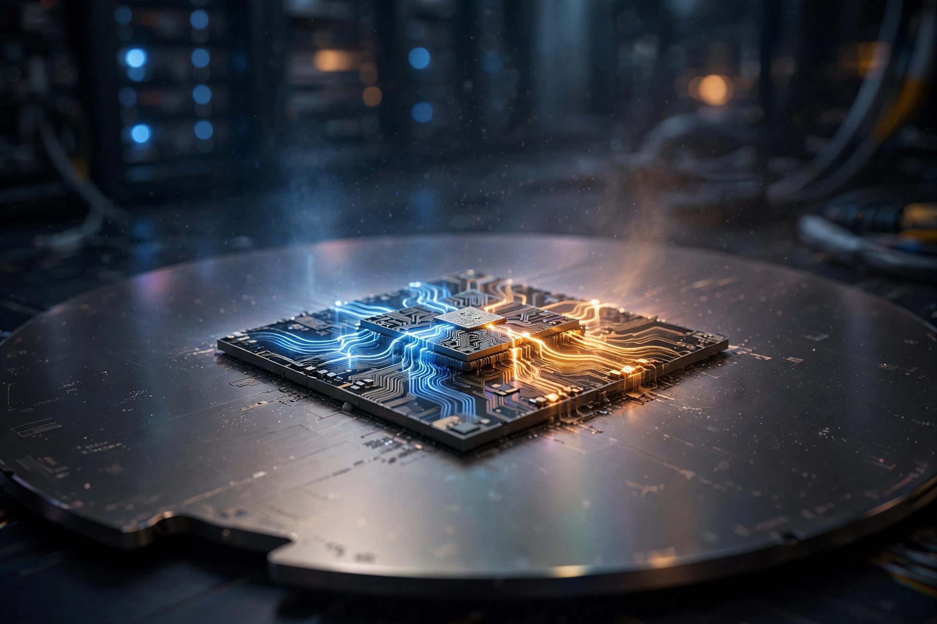
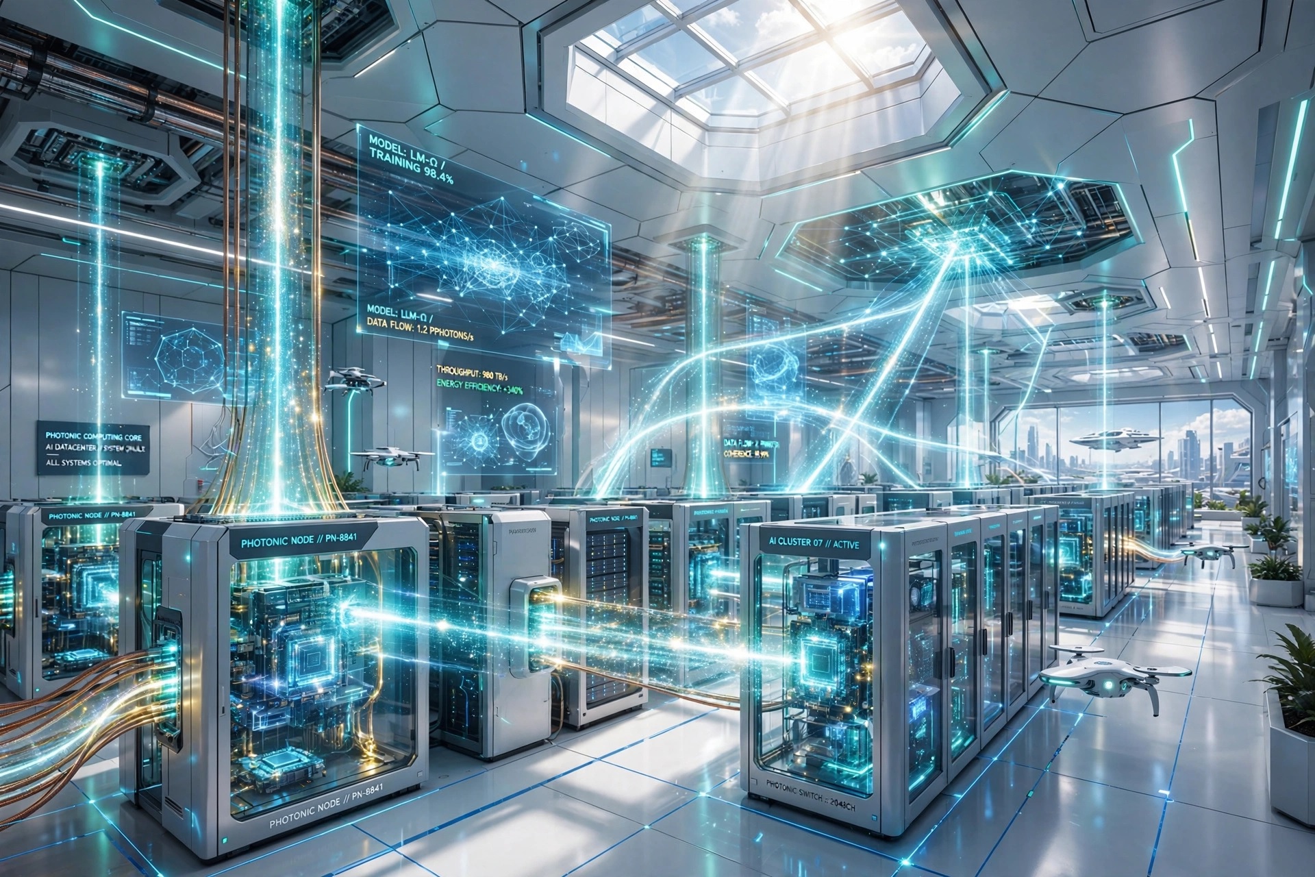
Inside a next-gen AI datacenter, racks no longer hum with hot copper cables — they glow with light. Photonic chips are about to do what Moore’s Law couldn’t.
Meta description: Discover how photonic computing and optical NPUs use light to accelerate AI, reduce chip heat, improve data-center efficiency, and reshape the future beyond traditional GPUs.
Executive Summary
Photonic computing uses light—not just electricity—to move and process information. Optical neural processing units, or optical NPUs, are designed to accelerate the math behind artificial intelligence by sending photons through tiny on-chip waveguides, interferometers, modulators, and detectors. The value is easy to understand: more AI throughput, less electrical resistance, lower heat, and potentially much better energy efficiency for inference-heavy workloads. This technology will not replace GPUs overnight. However, it could become one of the most important upgrades for AI data centers as power use, cooling, and chip-to-chip bandwidth become major limits on AI growth.
Hero:
Keywords: photonic computing, optical NPU, photonic chips for AI, silicon photonics, Lightmatter, optical neural network, AI datacenter energy efficiency, GPU overheating solution, optical computing explained
Executive Summary
For 70 years we computed with electrons. The future will compute with photons. A Photonic NPU (Neural Processing Unit) replaces transistors with light traveling through silicon waveguides to perform AI math at literal light speed—the result: 10x lower energy, near-zero heat, and terabit bandwidth. With companies like Lightmatter, Celestial AI (now acquired by Marvell for $3.25B), Ayar Labs, and Lightelligence raising over $1.5B in combined funding, photonic computing is moving from the lab to the datacenter in 2025-2026. This post explains what it is, how it works, how it’s made, who is building it, and why it will rewrite the rules of AI infrastructure.
What Is Photonic Computing/ Optical NPU?
Traditional chips compute by moving electrons through transistors and metal wires. That approach is powerful and proven, but it also creates waste heat because electrical resistance turns part of the energy into thermal load. Photonic computing moves selected tasks into the optical domain. Instead of representing values only as electrical signals, data can be encoded in light using intensity, phase, wavelength, or polarization. For AI, the main target is matrix multiplication—the repeated math operation at the heart of neural networks. Because light can split, combine, interfere, and travel in parallel, it offers a promising path to faster AI calculations with less heat at the point of computation.
How Optical NPUs Work – No PhD Needed
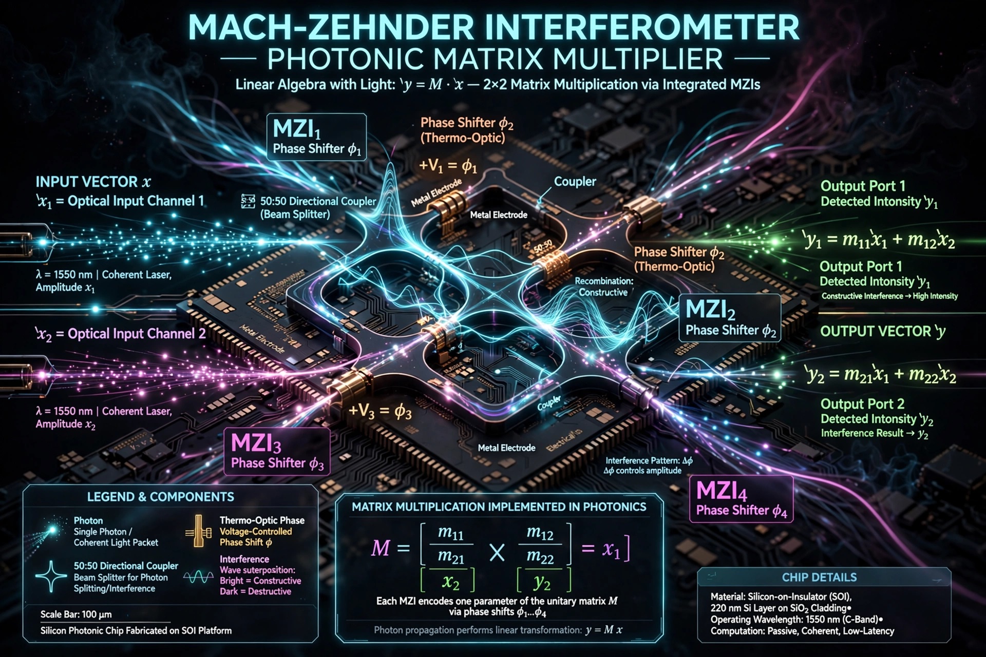
An optical NPU accelerates neural-network calculations by turning data into light, processing it through photonic circuits, and converting the result back into electrical signals when needed. A laser provides the light source. Modulators encode numbers onto beams of light. Waveguides act like tiny optical roads across the chip. Interferometers or ring resonators control how beams combine, which can represent neural-network weights. Photodetectors then read the output. In plain language, the chip lets physics do part of the math while light is moving, rather than forcing every operation through heat-producing electronic switching.
Inside a photonic chip:
- Encode: A laser (1550 nm, telecom standard) is split into many colors. Your input data (an image, text token) modulates the brightness of each color.
- Multiply: Light enters a mesh of Mach-Zehnder Interferometers (MZIs). Each MZI has tiny heaters that change the phase of light. By tuning the phase, you tune the “weight” of the neural network. When two beams meet, they interfere — constructively (add) or destructively (subtract). That’s multiplication.
- Accumulate: Multiple wavelengths travel in the same waveguide at once (Wavelength Division Multiplexing). A photodetector at the end sums all colors — that’s addition.
- Nonlinearity: The result is converted to a small electrical signal to apply ReLU/sigmoid, then converted back to light for the next layer.
Because this all happens at light speed in parallel, a single chip can reach >6000 TOPS (trillion operations per second), as demonstrated in 3D photonic chips in 2025
How Are Photonic Chips Made?
Most practical systems use silicon photonics, which adapts semiconductor manufacturing to build optical components on chips. Engineers pattern waveguides, couplers, modulators, thermal tuners, and detectors on wafers, then package them with lasers, electrical control circuits, memory, and high-speed I/O. The hardest parts are alignment, calibration, yield, heat from support electronics, and manufacturing repeatability. A photonic AI accelerator is rarely “all light.” It is usually a hybrid system: optics handle selected high-throughput math and communication, while electronics manage memory, control logic, nonlinear functions, and software compatibility.
They look like normal chips because they ARE made like normal chips:
- Material: Silicon-on-Insulator (SOI) wafer — 220nm silicon on oxide
- Process: Standard CMOS foundry (GlobalFoundries, TSMC) with added photonics steps. Waveguides are etched, not copper wires.
- Key Components: lasers, grating couplers, directional couplers (beam splitters), phase shifters (thermo-optic or electro-optic), photodiodes.
- Packaging: The hard part. Need fiber attach, laser co-packaging, and temperature control. This is where Co-Packaged Optics (CPO) comes in — Lightmatter’s Passage and Ayar Labs’ TeraPHY directly integrate optics next to the GPU/ASIC.
- Memory: New electro-optic analog memory holds weights without constantly burning power
Why This Could Reduce GPU Overheating
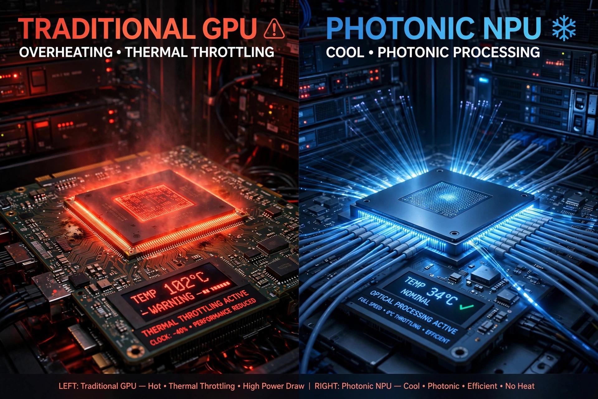
GPUs overheat because AI workloads push huge amounts of electrical current through dense transistor arrays and memory systems. Optical NPUs can reduce thermal pressure in two main ways. First, photons can carry information with far less resistive loss than electrons moving through copper wires. Second, some optical matrix operations can happen while light travels through passive or low-power structures. This does not remove all heat—lasers, drivers, memory, and electronic conversions still use energy—but it can make AI inference cooler and more efficient. In the near term, optical interconnects may deliver the biggest gains by reducing the energy cost of moving data between chips. Over time, optical compute engines could also reduce the heat created by neural-network math itself.
Key Benefits at a Glance
- Lower heat from reduced resistive electrical losses in selected compute and communication paths.
- Massive parallelism through wavelength-division multiplexing, where multiple colors of light carry data at once.
- High bandwidth for chip-to-chip and rack-scale AI systems.
- Potentially lower energy per inference for large AI models.
- Better sustainability for data centers facing power and cooling constraints.
Applications: Where Light-Powered AI Fits Best
Photonic accelerators are especially promising for AI inference, where trained models answer questions, generate images, translate text, detect fraud, recommend products, or control robots in real time. They may also help with scientific simulation, wireless signal processing, cybersecurity analytics, autonomous vehicles, medical imaging, and edge devices that need fast decisions without large batteries. In data centers, optical interconnects can move information between GPUs, CPUs, memory pools, and AI accelerators more efficiently. That matters because modern AI often spends more energy moving data than doing the actual math.
- AI chatbots and copilots: faster, cooler inference for large language models serving millions of users.
- Image, video, and voice generation: high-throughput acceleration for creative AI tools and media pipelines.
- Recommendation engines: lower-latency personalization for shopping, streaming, search, and social platforms.
- Fraud detection: real-time pattern recognition for banking, payments, insurance, and cybersecurity teams.
- Medical imaging: faster analysis of scans, pathology images, and diagnostic support systems.
- Autonomous vehicles and robotics: low-latency perception and decision-making for cameras, lidar, and sensor fusion.
- Telecom and 6G networks: rapid signal processing, beamforming, and network optimization.
- Scientific research: acceleration for physics simulations, climate modeling, genomics, and drug discovery.
- Edge AI: energy-efficient intelligence in factories, drones, smart cameras, satellites, and remote sensors.
- AI data-center networking: optical links that reduce bottlenecks between accelerators, memory, and storage.
Companies Building the Photonic Future
Several companies are pushing pieces of the optical AI stack forward. Lightmatter is known for photonic interconnect and photonic AI processor work. Ayar Labs focuses on optical I/O that can connect chips with extremely high bandwidth. Celestial AI is developing photonic fabric technology for AI infrastructure. Lightelligence has explored optical computing for AI acceleration. Luminous Computing has worked on photonic approaches to AI supercomputing. Q.ANT is developing photonic processing technologies in Europe. The broader ecosystem also includes foundries, laser suppliers, packaging specialists, and hyperscale data-center operators that may adopt optical links before full optical compute becomes common.
How Close Is Mainstream Adoption?
Photonic computing is moving from research labs into serious commercialization, but mainstream adoption will happen in stages. Optical interconnects are the closest opportunity because data movement is already a major bottleneck in AI clusters. Hybrid photonic-electronic accelerators may follow for specialized inference workloads where high throughput and low energy use justify new software and integration work. A full replacement for GPUs is unlikely in the short term because GPUs have mature tools, strong developer support, and flexible training capabilities. A realistic path is optical I/O and photonic fabrics expanding through the late 2020s, followed by broader optical NPU deployment in hyperscale inference, scientific computing, and low-latency mission-critical systems.
How to Apply Photonic AI in Real Projects
- Start with inference workloads where energy cost, latency, or bandwidth is the biggest constraint.
- Measure total system power, not only chip performance, including memory, networking, and cooling.
- Use photonic interconnects first if full optical compute is not yet practical.
- Plan for hybrid software stacks that combine GPUs, CPUs, conventional AI accelerators, and photonic modules.
- Track vendor roadmaps, foundry readiness, packaging quality, and model compatibility before committing at scale.
Conclusion: The Revolution Is Real—but Hybrid
Photonic computing is not magic, and it will not instantly solve every data-center cooling challenge. But it addresses one of AI’s most urgent problems: the rising energy cost of moving and processing data. Optical NPUs and photonic interconnects could help data centers deliver more intelligence per watt, lower heat density, and make large-scale AI more sustainable. The most likely winners will be hybrid systems that combine the flexibility of electronics with the speed and efficiency of light. In the next era of AI hardware, the key question may shift from “How many GPUs can we add?” to “How much of the workload can we move at the speed of light?”
FAQ: Photonic Computing and Optical NPUs
What is photonic computing in simple terms?
Photonic computing is a way of processing or moving information using light. Instead of relying only on electrical signals, it uses photons to carry data through tiny optical pathways on a chip.
Will optical NPUs replace GPUs?
Not immediately. GPUs are still highly flexible and supported by mature software. Optical NPUs are more likely to appear first as specialized accelerators or as part of hybrid systems that combine electronics and photonics.
How can photonic chips reduce overheating?
They can reduce heat by moving data with light, which avoids some of the resistive losses caused by electrical current in metal wires. Some optical operations can also happen as light passes through passive structures, lowering the energy required for selected AI calculations.
What are optical NPUs best used for?
They are especially promising for AI inference, high-speed data movement, recommendation engines, generative AI, medical imaging, telecom signal processing, edge AI, robotics, and scientific simulations.
When will photonic computing become mainstream?
Mainstream adoption will likely happen gradually. Optical interconnects may scale first in AI data centers, followed by hybrid photonic-electronic accelerators for specialized inference workloads later in the decade.
References
- “Universal photonic artificial intelligence acceleration.” 2025.
- Torrijos-Morán, L., Pérez-López, D. Industry insight: photonics to scale AI data centers. npj Nanophoton. 3, 8 (2026). https://doi.org/10.1038/s44310-025-00105-1
- Ayar Labs. “Optical I/O and silicon photonics resources.” Company technical materials.
- “Photonic computing and AI infrastructure resources.” Company technical materials.
- IEEE and SPIE technical literature on silicon photonics, optical interconnects, and photonic AI accelerators.
In Belo Jardim, student of the Grupo Escolar Bento Américo and Prof. Donino Gymnasium, and student of the teachers: Dulce Ramos, Alba Leite, Dona Conceição Moura, Dona Olindina Mergulhão, Estefânia Moura Bezerra, and Maria Luiza